Digital Electronics/Lecture Flip-flops
|
History
[edit | edit source]The first electronic flip-flop was invented in 1919 by William Eccles and F. W. Jordan [1]. It was initially called the Eccles-Jordan trigger circuit and consisted of two active elements (radio-tubes). The name flip-flop was later derived from the sound produced on a speaker connected with one of the backcoupled amplifiers output during the trigger process within the circuit. Note that this original flip-flop was transparent and thus probably would be labeled latch today (see here).
Design And Usage
[edit | edit source]
S R Latch
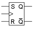
[edit | edit source]The S R Latch or set reset Latch is the root behind most flip flops.
One example of usage for this would be a simple security system. R is hooked up to a key to arm it and a trigger or switch on a door or window is hooked up to S to set it off.[2]
For devices with a clock input it may be needed to tie the clock high or low (active low clock pin).
2-6V (TI CD74HC112)
3-18V (TI CD4027)
| SR latch operation | |||
|---|---|---|---|
| S | R | Q | Q |
| 0 | 0 | Keep state | |
| 0 | 1 | 0 | 1 |
| 1 | 0 | 1 | 0 |
| 1 | 1 | Unstable condition | |
Logic Components
[edit | edit source]A SR latch is not a basic logic gate - rather it consists of 2 other NOR gates. The left most 2 NAND gates in the image below are only needed to add a clock functionality to the latch.

- Schematic for usage
- Different Devices
J K Flip Flop
[edit | edit source]
For the most part the J K flip flop is the same as a SR latch except that when both inputs are high the output will toggle with the clock rather than being an unstable state as with the SR latch.
Some flip flops also feature a preset and clear pin which operates asynchronously to the clock. Setting preset high will set Q high and clear will set Q clear regardless of the clock state.[1]
For devices with a clock input it may be needed to tie the clock high or low (active low clock pin).
2-6V (TI CD74HC112)
3-18V (TI CD4027)
| JK flip flop operation | |||
|---|---|---|---|
| J | K | Q | Q |
| 0 | 0 | Keep state | |
| 0 | 1 | 0 | 1 |
| 1 | 0 | 1 | 0 |
| 1 | 1 | Toggle with clocks rising edge. | |
logic components
[edit | edit source]
- Schematic for usage
- Different Devices
T Flip Flop
[edit | edit source]Toggle Flip Flop, an edge trigger flip flop. Assuming the input port named "T", controlling signal named "clk" and the output port named "Q"; then @edge of clk (positive edge or negative edge according to flip flop design) the output "Q" toggles its value iff input "T"='1' otherwise the output "Q" sustains its value.
| T-flip flop operation(positive edge) | |||
|---|---|---|---|
| clk | T | Q | Q |
| positive edge | 0 | Keep previous state | |
| positive edge | 1 | Toggle previous state | Toggle previous state |
| otherwise | 0 or 1 | Keep previous state | Keep previous state |
notice that the flip flop senses the "T" at the edge of "clk"; thus any changes occurs in "T" value at any other time is ignored
- logic components
it's a JK flip flop with "J" and "K" connected together to form the input "T"
- Schematic for usage
- Different Devices
D Flip Flop
[edit | edit source]An edge trigger flip flop. Assuming the input port named "D", controlling signal named "clk" and the output port named "Q"; then @edge of clk (positive edge or negative edge according to flip flop design) the output "Q" takes the value of the input "D"; otherwise the output "Q" sustains its value.
| D-flip flop operation(positive edge) | |||
|---|---|---|---|
| clk | D | Q | Q |
| positive edge | 0 | 0 | 1 |
| positive edge | 1 | 1 | 0 |
| otherwise | 0 or 1 | Keep previous state | Keep previous state |
notice that the flip flop senses the "D" at the edge of "clk"; thus any changes occurs in "D" value at any other time is ignored
- logic components
it's a JK flip flop with "J" connected to the input "D" and "K" connected to the inverted value of input "D".
- Schematic for usage
- Different Devices
Notes and references
[edit | edit source]https://en.wikibooks.org/wiki/Digital_Circuits/Latches
https://en.wikibooks.org/wiki/Digital_Circuits/Flip-Flops
| Resource type: this resource contains a lecture or lecture notes. |
