
Digital Circuit Lab
Week0 Activities
[edit | edit source]Write problem/project Goal
[edit | edit source]So I found a video of a team of students that built a robot that can balance on a ball. My goal is to emulate the functionality of their project (inexpensively). Additionally, it is worth noting that I am doing this outside of any class. It is my own project and is being done without the material support of the school. That being said, the general quality of the final project is expected to be lower for several reasons not the least of which is financial.
Of note: This is my first project in robotics and I am currently only a few weeks into a digital logic lab class. Having said that, assumptions I make in the beginning may vary widely in their accuracy and will improve both due to experience with the parameters and limitations of the project but also due to general experience with the design environment I will be working in.
My First Task
[edit | edit source]Research the various elements that go into a balancing robot.
- Materials: Chassis, electronics, code and wheels.
- Parts Research
-
 :Chassis Kits
 -
 :Prototyping board
 -
 :Standoff bars
 -
 :Wheels
 -
 :Higher End Wheels


Week1 Activities
[edit | edit source]My Second Task
[edit | edit source]The task I am giving myself this week is to become familiar with the accelerometer.
Week1 Narrative
[edit | edit source]The accelerometer
[edit | edit source]The Following is from an excelent guide and the only resource I have found useful in practical use of the accelerometer.
Analog accelerometers will output a voltage level within a predefined range that you have to convert to a digital value using an ADC (analog to digital converter) module. For example a 10-bit ADC module will output a value in the range of 0..1023, note that 1023 = 2^10 -1. A 12-bit ADC module will output a value in the range of 0..4095, note that 4095 = 2^12-1.
Let's move on by considering a simple example, suppose our 10bit ADC module gave us the following values for the three accelerometer channels (axes):
- AdcRx = 586
- AdcRy = 630
- AdcRz = 561
- Each ADC module will have a reference voltage, let's assume in our example it is 3.3V. To convert a 10bit adc value to voltage we use the following formula
- VoltsRx = AdcRx * Vref / 1023
- A quick note here
- that for 8bit ADC the last divider would be 255 = 2 ^ 8 -1 , and for 12bit ADC last divider would be 4095 = 2^12 -1.
- Applying this formula to all 3 channels we get
- VoltsRx = 586 * 3.3V / 1023 =~ 1.89V (we round all results to 2 decimal points)
- VoltsRy = 630 * 3.3V / 1023 =~ 2.03V
- VoltsRz = 561 * 3.3V / 1023 =~ 1.81V
- Each accelerometer has a zero-g voltage level, you can find it in specs, this is the voltage that corresponds to 0g. To get a signed voltage value we need to calculate the shift from this level. Let's say our 0g voltage level is VzeroG = 1.65V. We calculate the voltage shifts from zero-g voltage as follows
- :
- DeltaVoltsRx = 1.89V – 1.65V = 0.24V
- DeltaVoltsRy = 2.03V – 1.65V = 0.38V
- DeltaVoltsRz = 1.81V – 1.65V = 0.16V
- We now have our accelerometer readings in Volts , it's still not in g (9.8 m/s^2), to do the final conversion we apply the accelerometer sensitivity, usually expressed in mV/g. Lets say our Sensitivity = 478.5mV/g = 0.4785V/g. Sensitivity values can be found in accelerometer specifications. To get the final force values expressed in g we use the following formula
- Rx = DeltaVoltsRx / Sensitivity
- Rx = 0.24V / 0.4785V/g =~ 0.5g
- Ry = 0.38V / 0.4785V/g =~ 0.79g
- Rz = 0.16V / 0.4785V/g =~ 0.33g
- We could of course combine all steps in one formula, but I went through all the steps to make it clear how you go from ADC readings to a force vector component expressed in g.
- Rx = (AdcRx * Vref / 1023 – VzeroG) / Sensitivity (Eq.2)
- Ry = (AdcRy * Vref / 1023 – VzeroG) / Sensitivity
- Rz = (AdcRz * Vref / 1023 – VzeroG) / Sensitivity
The sensitivity of the accelerometer I am using from the Data Sheet is 420 mV/g or 0.420 V/g
- Playing with the Accelerometer
-
 :Accelerometer Setup
 -
 :Accelerometer_Readings


The chassis
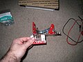
[edit | edit source]The wife, being much smarter than myself decided to post on freecycle a request for an erector set. A very nice woman happened to have one to give me so the hunt for materials to construct a chassis was made significantly easier. A quick trip to the hardware store for nuts and bolts and i was able to put together a nice little chassis. The design in the above referenced video operated three servos so as a starting point I am going to go with that. Also, three is cheaper than four so.
- Playing with the Accelerometer
-
 :Erector Set
 -
 :Front veiw
 -
 :Back veiw
 -
 :Side veiw
 -
 :Underside of chassis


Because I am going with three wheels and it is a square design I needed to compensate for the uneven support. I put the weight in the front where there are two legs to take the brunt of the weight. On the back with only a single leg and two unsupported edges was added support braces, which do nothing for the tendency of those edges to tip the structure over but keeps the platform level under light pressure. I am sure that adjustments will need to be made as the design process continues. It is possible that the square design will need to be abandoned all together, but we will see.
Additional
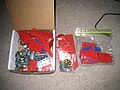
[edit | edit source]I also put an order in for necessary parts.
-ADC (analog to digital converter) if I am going to end up using the nexys2 as my micro-controller board (overkill I know) I will need this. For this i ordered the PMOD ADC from digilent, slightly more expensive but easy to work with.
-Servo motor, These have a gear box that can be modified to decrease torque increase RPM as appropriate. It voids the warranty but who cares.
-Servo Connector for the nexys2. I could have done without this, just a convenience factor for connecting/controlling multiple servos from the same port.
Week2 Activities
[edit | edit source]My Third task
[edit | edit source]Since the parts I ordered are not going to be here until early next week, my task for this week is simple: research.
Week2 Narrative
[edit | edit source]I have found a couple of very good resources of information on theory and practical implementation of the ballbot. One in particular is from LUND University outlining their building of a similar project. The following images are from the LUND Univeristy project illustrating their models motion control mechanism.
- Wheels and Balls
-
 :Wheel to ball implementation
 -
 :Omni wheel control
 -
:Omni Wheels


This primarily demonstrates what I had feared, that my crude chassis would need a total revamp. Firstly I decided to go with the servo motor alignment and let the rest build from there, since the motor alignment seems to be important to creating an understandable way to control the ball. The following images are what I came up with, they may still need further adjustments. I also ended up buying a set of omni wheels shown in the image gallery above.
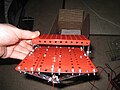
- Reimagined Chassis
-
 :120 degree separation bar
 -
 :Servo Motor Holder
 -
 :Assembled, bottom view
 -
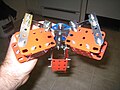 :Side veiw
 -


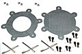
The Upper portion of the chassis will be constructed from a circular prototyping plate show above. It is 140mm in diameter (6.69 inches). This was actually fairly difficult to find to the specifications I wanted. The diagonal length of the Nexys2 is 6.5 inches and I wanted a chassis that could accomidate this without having the board flow over. Also because I went will prototyping board I can easily connect the Nexys2 with standoff bars. Also for reference, the length from the center bolt to the end of each arm of the 120 degree separation bar is 3.25 inches. More measurements will need to be taken when the servos and wheel arive to determine weather adjustments need to be made but for now the nearly 7 in diameter chassis seems to be a nice fit with a little wiggle room for modifactions to the servo placements.
Week3 Activities
[edit | edit source]My Fourth task
[edit | edit source]My servos and some other random parts came in so my task for this weekend is to create the test platform that will eventually become the base of the robot. I have been reading up on the controlling a servo and believe I have a fairly good understanding of how to implement it in the FPGA.
Week3 Narrative
[edit | edit source]Both the creation of the test platform and the programming of the FPGA for servo motor interface is done. I have created a video demonstration of the platform in action. The main problem I am having so far is that the FPGA can only reliably control 2 servo motors at the same time. If I have three going then it apps to lose power and restart. I believe that this will be corrected with an external power source. I believe in the final implementation there will be two external power sources one for the board which I have tested crudely but it works. The second will be for the servos only
|

I have yet to create an algorithm for handing control to the accelerometer, but I might have to let that one go until next weekend. So to control the servo you send a pulse of varying width to the servo every 20 ms. The width determines the position the servo goes to. I discovered that technically I have controlled motors rather than servos because they spin 360 degrees. The width in this case simply designated direction. This may make it somewhat more difficult to control (maybe not, we will see) but is necessary because I will want to give the robot mobility once I have all the basic functionality done.
Week4 Activities
[edit | edit source]Week4 Narrative
[edit | edit source]This weekend I have been trying to some frustration to create a I2C Master protocol for my Nexys2 FPGA so that I can talk to my accelerometer and have its readings control to servo motors. I2C is a 2 wire communication protocol common in modern electronics. It consists of a bidirectional data wire (SDA line) and a synchronous clock(SCL line) to time the back and forth. The data sheet and manual for the adc and I2C chip within the adc call for the following:
- a start condition: this consists of a period where SDA transitions from high to low during the SCL high period. This condition alerts the I2C slave device that a device address is coming and the Slave device powers on and waits.
- a device address, the address in this case is 0101000 followed by either a 1 if I intend to read from the device or a 0 if I intend to write to its register. The register sets up to 4 channels to convert its analog input to digital output to report to the I2C master. The next bit the slave pulls the SDA line to 0 to indicate the address has been accepted.
- Next I write the 8 bits of register settings to determine which channels I wish to have converted, this is followed by another slave ack bit.
- At this point I do a stop condition followed by an imediate start condition.
- again I send the address but here I follow with a 1 to indicate read is intended. This is followed by an ack from the slave device.
- 1 byte of data is sent from the slave device, 2 zeros and 2 channel indicators to indicate which of the up to 4 channels is being sent out, then the 4 MSB of the 12 bit ADC data. This is followed by the master ACK bit where the master pulls the SDA line to zero to indicate reception of data. Then another byte consisting of the remaining 8 bits of ADC data followed by another master ACK bit.
- If another read is intended a repeated start condition should be done. This is the same as the previous start only no address is needed, just start and another 2 bytes. This happens until the master sends a NOACK bit, that is leaves the SDA line high during the ACK bit.
- I2C protocol
-
 Start condition
 -
 Stop condition
 -
 Phase Two of I2C protocol


Above is an image of the start and stop conditions described. Also is an image of the whole process shown in the test bench. The process is a finite state machine controlled by a clock 4x faster then the SCL. This allows the shift in SDA to occure while SCL remains high and also allows for all other processes to happen at the falling edge of the SCL. This last is important because a inadvertant transition of SDA while SCL is high can signal a stop condition and break communication with the I2C slave. It should also be noted that in the test bench SDA line is blue and only raised half way. This is because SDA is set to 0 or Z. Z being high impedance, this condition allows for either device to drive the line low if appropiate. It is pulled up to logical 1 while in Z condition by an external resistor. Assentialy making the SDA line always high unless one of the devices pulls it low.
Above is an image of the 2 clocks, SCL used to sync the signal to the slave device and the stateCLK I use to drive the FSM. Also shown above is an image of the SDA line and SCL line together. This image shows an error in FSM that I have yet to correct. Currently it produces an endless stream of write addresses. Correcting this will be difficult as I have combed my code and cannot readily see why it does that, combined with the test bench showing that it should produce what I want has left me perplexed. This though will be next weekends job.
Week5 Activities
[edit | edit source]So I have the ADC and Accelerometer working but I am having trouble with channel bleed. Both X-axis and Y-axis data is being recorded on both channels. I suspect it is something to do with how I am handling the input, but we will see. My first thought is that I can Mux the register settings and take a single sample of a single channel then stop and take another sample of the other channel. It data is only used every 20 ms and it only takes 442 us to take a reading so this shouldnt be a problem.
Week5 Narrative
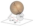
[edit | edit source]So as I suspected the bleed through was just how I was handling the input. I now test the channel indicator before I record the data rather than after. I believe it was causing timing issues recording some data then as the indicator bit changed recording the rest on the other register causing a hodge podge of both axis on both registers. So far I have created a couple of simple drawings to illustrate my initial concepts for servo control.
|


In the tilt angle sensitivity image above I have worked out through experimentation that the actual range of sensitivity I am concerned about is much smaller. If the robot were to tilt beyond the range of the inner circle it would surely tip over. Also I found that the nominal values of x-axis and y-axis are not (nor were they expected to be) pitch perfect, but they are also a fair bit different. A closer representation of the control logic will be needed before I can continue to much farther.
- Revised Passive Control Logic
-
 Motor Speed Control Added

So a bit about the revision to the servo control, I created stages of sensitivity where the servo motor logic is the same if tilting in the same direction, but one or more motors will be operating at higher speeds depending on the level of tilt. The speeds I have chosen for each stage, while not arbitrary, are experimental values that will almost certainly be changed before much longer. I have implemented the revised servo control algorithm and it does appear to be working as intended. I sort of need the prototyping plates to arrive so I can put this thing together. Trying to test the algorithm where everything is just lose wires hanging off a board makes it difficult to maintain proper control of everything. Because of this no measurements are currently possible. If I get froggy I may try to figure out how to create a video component that would track the movement and be able to compare this to current acceleration data. That would be interesting, but I think that would have to be a back seat problem at the moment. My ambition for this project is weighing heavily on the actual work I am expected to do for school.
Week6 Activities
[edit | edit source]The prototyping plates came in and while I didn't have time to do any extensive testing I could see that the speed choices I made for the algorithm were way off. I think that a very small speed to start within the first range within my control logic diagram I made last week and a swift increase to say 75% of full. Also I have been doing research into math machines that can be built with the FPGA that may be useful in creating a smother control function. I am kinda glad I picked this as my first project because it is forcing me to learn way more than I would have needed to with something simpler.
Week6 Narrative
[edit | edit source]So getting everything together and starting to test I see that the accelerometer is producing huge spikes. I have the LEDs showing accelerometer data. My first thought is that I need to rework my algorithm, as it turns out this is true but not in the way I was thinking. Doing some research lead me to find that I need to incorporate a gyro into the design. This is because accelerometers measure acceleration. That is it measures gravity while at rest and total acceleration while in motion. A gyro used in conjunction to the accelerometer will smooth out the accelerometer readings while moving.
This is done using a filter to take into account current accelerometer data with past accelerometer + gryo correction and a prediction of future position. Here is an excellent tutorial on the subject I found. So I have placed an order for a 3 axis gyro, a small breadboard so that I can stop using the one I have for class. This way I dont have to take apart my project when I convince myself to do homework, and some 6 pin connectors. Unfortunately I don't think I will get much done this week save for possible changing my I2C state machine to accommodate a second slave. I might also start writing up some code for the filter described above.